Test of Version 1 Digitizers
The first generation of the Tilecal digitizer and Slink interface has been tested. Numerous Data has been taken using 3in1 card CIS signals, among them there was data failure problem, this note try to describe the pattern of the data failure observed.
Readout protocol of the first generation digitizer
.A complete data package of L1A event include following informations:
First the control word comes, this indicates that a new event data package begins, after that it is a data block that contains the data comes from all channels of every digitizer board present, then another control word conclude the data package at the end.
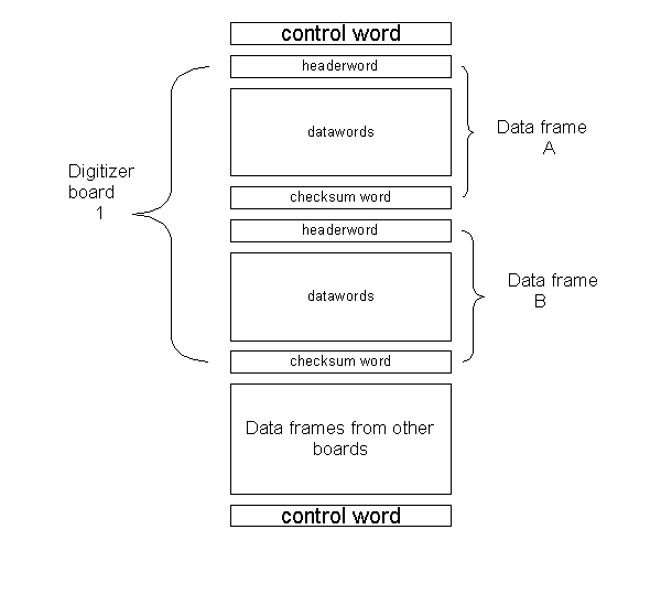
In the data block, there are data frames. The number of the data frame depends on how many digitizer board present in the readout system, one more digitizer board means two more data frames, because each digitizer contributes two data frames to the data package, say Data frame A and Data frame B, Data frame A consists data from ADC channel 1, 3, and 5, while Data frame B consists data from ADC channel 2, 4, 6. In the data block, the Data frame A of first digitizer board always comes first, then the Data frame B; then the data from other boards, one digitizer board by one digitizer board, each of them has Data frame A and Data frame B.
Within the data frame, it begins with headerword which consists the necessary information of the data frame, the highest bit bit31 of the DWORD headerword is 1, which make the headword can be distinguished from the dataword whose highest bit is 0. The headerword is followed by a number of datawords; the number of the datawords is predefined by program. At last a checksum word ends the data frame.
Dataword is 32bit unsigned long int, highest bit bit31 is dataword flag which is 0, bit30 is even parity bit, bit29-bit20, bit19-bit10, bit9-bit0 are data of 10-bits-ADC channel 1, 3, 5 for Data frame A or 2, 4, 6 for Data frame B respectively.
Data lost instead of data wrong
During the test, 3in1 card's CIS signal was connected to the ADC input terminal on digitizer board. The digitizer board were setup as run mode, sample number 15, pipeline 100. 22 events were investigated.
From the data acquired, the parity check is correct among all more than one thousand dataword, which suggested that the data received are correct. But the number of data received is less than the number we expected, and the possibility of lost of different type data is not the same. The first control word was most liable to lost than other data. We list the result of investigation at the table bellow.
Table. Data lost statistics
|
Data catalogue |
Expected Number |
Received |
Lost |
Lost possibility |
|
1st control word |
22 |
7 |
15 |
68% |
|
Head word |
88 |
82 |
6 |
7% |
|
Data word |
1320 |
1264 |
56 |
4% |
|
Checksum word |
88 |
37 |
51 |
58% |
|
Last control word |
22 |
21 |
1 |
5% |
Why data lost
The reason why data lost is far deeply inhabited in the design architecture and strategy of digitizer board and Slink interface board.
We have investigated the output digital signal from digitizer board at the input port of Slink interface card, using HP 1670 250MHZ digital analyzer. The result shows that some of those signals are far from stable, and some data pulse are only half width of normal data pulse.
Also, the mal_manufactured Slink interface card make the data package more liable to lost data.